 |
 |
 |
|
|
|
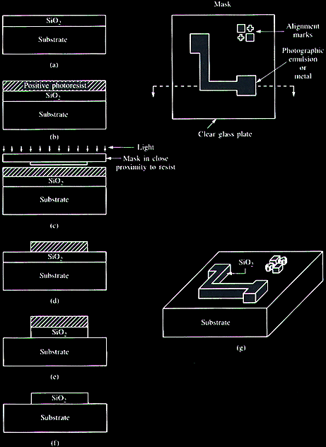
Lithography is the process in which a microelectronics patterns are transfer to a substrate. This transfer can be aided by light, electron-beams, ion beams, x-rays, etc. Shown below is a typical contact photolithography procedure:
Pattern Layout and Generation
This is typically 100-2000 times the final size.
Resist Requirements
Sensitivity - high sensisity reduces exposure time
Adhesion - resist must adhere to the surface and
not lift-off
Fabrication properties - etch resistance, temperature
stability.
Resolution - what linewidth can we achieve?
Resist removal, rinse, and dry.
Resolution limit = 106 / (l x
fnumber)
where l is the wavelength
in nanometers f-number of the lens.
Today, we have computer aided design which has provided a new medium for the layout of microelectronic circuits. These systems are all based on interactive graphic packages. The output of the CAD system is usually in the form of digital information stored on a magnetic tape. The tape can control photoplotter or an e-beam lithography system.